






- This topic is empty.
-
AuthorPosts
-
2026-11-05 at 4:16 pm #18284
A Depth-Controlled Rigid-Flex PCB combines rigid circuit sections with flexible interconnects while requiring selected manufacturing operations to stop at a precisely defined depth. This approach can support compact electronic assemblies, controlled-depth cavities, localized material removal, and complex board structures where conventional full-depth drilling or routing is unsuitable. Achieving reliable results depends on more than the nominal board thickness: layer stack-up, copper distribution, dielectric properties, tooling accuracy, and the relationship between rigid and flexible sections must all be considered during design and manufacturing.
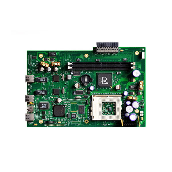
For applications such as medical electronics, automotive control systems, industrial instrumentation, and compact communication equipment, depth-controlled processing can influence mechanical fit, electrical performance, and long-term reliability. The key is to define exactly which layer or material interface must remain intact, then establish a manufacturing process capable of achieving that result consistently.
Shenzhen Rongbaijia Technology Co., Ltd., established in 2009, provides PCB manufacturing and one-stop PCBA services, including multilayer, HDI, flexible, rigid-flex, high-frequency, and high-speed boards. Its engineering support and design-for-manufacturability (DFM) capabilities provide a useful foundation for evaluating complex PCB structures from initial design through assembly.
What Does Depth Control Mean in Rigid-Flex PCB Manufacturing?
In PCB fabrication, depth control refers to regulating the depth of a machining operation rather than cutting or drilling completely through the board. Depending on the design, the process may involve controlled-depth routing, counterboring, cavity formation, or other localized material-removal operations. These processes are not interchangeable, and the appropriate method depends on the intended structure.
For a rigid-flex design, the challenge is greater because the board contains regions with different material systems and mechanical behavior. Rigid sections commonly use reinforced dielectric materials, while flexible sections use thin polymer films and copper layers. Adhesives, coverlays, bonding films, and copper distribution can further complicate the stack-up.
A controlled-depth operation must therefore be evaluated against the actual layer structure. If a cavity is intended to stop above a copper layer, excessive depth may damage the conductor or compromise electrical isolation. If the process removes too little material, the remaining structure may interfere with component clearance, connector seating, or mechanical assembly.
The engineering drawing should identify the operation, reference surface, target depth, tolerance, and any layers or materials that must not be penetrated. Where the required depth is referenced to a finished surface, the specification should account for relevant surface finishes and thickness variation. Defining these details early reduces ambiguity during fabrication.
Stack-Up Design Determines Process Feasibility
The stack-up is one of the most important inputs for a Depth-Controlled Rigid-Flex PCB. It establishes the sequence and thickness of copper, dielectric materials, flexible films, bonding layers, coverlays, and other structural elements. Even when the overall board thickness is known, local thickness can vary between rigid and flexible regions.
This matters because a depth-controlled operation is performed relative to a physical reference surface, while the critical interface may lie beneath several materials with different thickness tolerances. A nominal depth alone may not provide sufficient assurance that the intended layer will remain intact.
For example, consider a design requiring a shallow cavity in a rigid section to create component clearance. The target depth must be assessed against the local copper and dielectric arrangement, not simply the total thickness of the board. If the cavity approaches a conductor, the residual dielectric thickness becomes a critical design parameter. The allowable minimum must be established according to the electrical requirements and the manufacturing process.
Depth tolerance should be selected in relation to the function of the feature. A non-electrical clearance pocket may permit a different tolerance from a cavity that approaches a copper layer or supports a tightly constrained mechanical interface. Tighter tolerances can increase inspection requirements, process complexity, and manufacturing cost, so they should be driven by documented functional needs.
The stack-up should also identify rigid-to-flex transition areas and keep depth-controlled machining away from sensitive transitions unless the process has been specifically validated. Abrupt changes in thickness and material stiffness can create local stress concentrations, particularly when the assembly is subjected to repeated flexing or vibration.
Tooling Accuracy and Material Removal
The achievable depth depends on the machining method, equipment condition, tool geometry, workholding, and material characteristics. Mechanical routing, controlled-depth drilling, and specialized cavity processes each have different limitations. The correct choice should be made from the feature geometry and the materials being removed, rather than from the assumption that one method suits every rigid-flex design.
Tool wear can change cutting behavior and affect dimensional repeatability. Workpiece flatness and fixture stability can also influence the relationship between the tool and the board surface. If the board is not held consistently, a nominally accurate machine setting may not produce a uniform cavity depth across the panel.
Rigid-flex constructions introduce additional variables because different materials can respond differently during machining. Resin systems, copper layers, flexible films, and bonding materials may have different cutting characteristics. Tool selection and process parameters should therefore be qualified using the actual material stack.
Where a depth-controlled feature approaches a conductive layer, the process should be validated through representative coupons or other suitable inspection methods. Cross-sectional analysis can help verify the remaining dielectric thickness and identify unintended copper exposure or material damage. The inspection method should match the feature's risk and the required acceptance criteria.
Electrical and Mechanical Reliability Considerations
A depth-controlled feature can affect electrical reliability even when it does not visibly damage the board. If the operation reduces dielectric thickness beneath a conductor, the resulting structure may no longer meet the intended insulation requirements. If copper is exposed or partially removed, the board may experience electrical discontinuity, shorts, or reduced resistance to environmental stress.
The design should therefore establish minimum residual material requirements and define prohibited conditions, such as exposed copper where insulation is required. Electrical testing remains important, but it does not replace dimensional verification when the critical risk is excessive material removal.
Mechanical reliability is equally important in rigid-flex products. The flexible region may experience bending during installation or throughout product operation. Routing or cavity features near the rigid-flex transition can influence local stiffness and stress distribution. A design that passes initial electrical testing may still fail under repeated movement if the flexible section is constrained or damaged.
Bend radius, copper construction, flex-layer orientation, adhesive behavior, and the location of stiffeners should be reviewed together. Dynamic-flex applications generally need more conservative design validation than assemblies where the flex section bends only during installation. Depth-controlled operations should not unintentionally reduce the structural support needed around components, connectors, or mounting points.
DFM Review Before Prototype Release
A structured DFM review can identify depth-control risks before fabrication begins. The review should examine the stack-up, local thickness, target depth, tolerance, tool access, feature-to-copper clearance, and proximity to rigid-flex transitions. It should also determine whether the feature can be inspected reliably after fabrication.
Manufacturing drawings should distinguish between nominal board thickness and local thickness at the machining location. They should state the measurement datum, the required depth tolerance, the minimum remaining material where relevant, and whether any copper or dielectric interface must remain untouched.
If the design is still flexible, alternative approaches may be worth comparing. Moving a component, changing the local stack-up, using a different mechanical clearance strategy, or revising the cavity geometry may achieve the same functional objective with less manufacturing risk. The most economical solution is often the one that avoids unnecessary precision requirements rather than simply tightening process tolerances.
Rongbaijia's PCB and PCBA services include engineering support and DFM analysis. For a specific Depth-Controlled Rigid-Flex PCB project, the manufacturer should confirm the available depth-control processes, achievable tolerances, inspection methods, and material compatibility against the actual design.
Quality Control from Fabrication to Assembly
Depth-controlled features should be included in the inspection plan as defined characteristics rather than treated as ordinary routing details. Depending on the application, verification may include depth measurements, dimensional inspection, cross-sections, electrical testing, and visual examination for delamination, burrs, or unintended copper exposure.
First-article inspection is particularly useful when a new stack-up or cavity geometry is introduced. Representative coupons can help establish the relationship between machine settings and finished dimensions before the process is released for volume production. Subsequent inspections should confirm that critical characteristics remain within the agreed limits.
For assembled boards, the review should also consider whether the cavity provides the intended component clearance and whether assembly operations introduce mechanical stress. Where the rigid-flex board will be integrated into a finished electronic product, PCBA testing can provide additional evidence of functional performance.
Rongbaijia reports capabilities including multilayer PCB production, HDI manufacturing, automated optical inspection, flying-probe testing, and PCBA services with SMT, through-hole soldering, and ICT/FCT testing. The exact inspection and testing plan for a Depth-Controlled Rigid-Flex PCB should be agreed upon according to the product's electrical, mechanical, and regulatory requirements.
A successful design combines a clearly defined depth-controlled feature with a manufacturable stack-up, validated machining parameters, and measurable acceptance criteria. By addressing these factors before prototype release, developers can reduce fabrication risk, improve repeatability, and create a more reliable path from initial samples to production.
http://www.rbjpcb.com
Shenzhen Rongbaijia Technology Co., Ltd. -
AuthorPosts

- You must be logged in to reply to this topic.